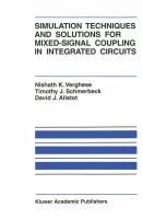
Simulation Techniques and Solutions for Mixed-Signal Coupling in Integrated Circuits
- List Price: $249.00
- Binding: Hardcover
- Publisher: Kluwer Academic Pub
- Publish date: 03/01/1995
Description:
1 Introduction.- 2 Sources of Noise and Methods of Coupling.- 2.1 Semiconductor Device Noise and Phenomena.- 2.2 Noise from Switching Voltage and Current.- 2.3 Inductive Coupling.- 2.4 Capacitive Coupling.- 2.5 Substrate Coupling.- 2.6 Summary.- 3 Semiconductor Device Simulation.- 3.1 Significance.- 3.2 Basic Equations.- 3.3 Boundary Conditions.- 3.4 Models of Physical Parameters.- 3.5 Spatial Discretization.- 3.6 Solution Methods.- 3.7 A Representative Example.- 3.8 Summary.- 4 Simplified Substrate Modeling and Rapid Simulation.- 4.1 Simplified Equation.- 4.2 Spatial Discretization.- 4.3 Boundary Conditions.- 4.4 Solution Methods.- 4.5 Asymptotic Waveform Evaluation (AWE).- 4.6 Substrate AWE Macromodels.- 4.7 Transient Simulation of AWE Macromodels.- 4.8 Substrate DC Macromodels.- 4.9 Matrix Solution.- 4.10 Results.- 4.11 Summary.- 5 Mesh Generation.- 5.1 Adaptive Mesh Refinement.- 5.2 A Priori Mesh Refinement.- 5.3 Summary.- 6 Substrate Modeling in Heavily-Doped Bulk Processes.- 6.1 Motivation.- 6.2 Single Node Substrate Model.- 6.3 Modified Single Node Substrate Model.- 6.4 Summary.- 7 Substrate Resistance Extraction for Large Circuits.- 7.1 Nested Macromodeling.- 7.2 Interpolated Macromodeling.- 7.3 Summary.- 8 Modeling Chip/Package Power Distribution.- 8.1 Effect of Power Bus Structure on Noise coupling.- 8.2 Summary.- 9 Controlling Substrate Coupling in Heavily-Doped Bulk Processes.- 9.1 Characterization of noise coupling concepts.- 9.2 P+ Bulk Wafer Characterization.- 9.3 Effect of Substrate contact placement on coupled noise.- 9.4 Effect of Package Inductance on Substrate noise.- 9.5 Noise Coupling Control Techniques.- 9.6 Summary.- 10 Controlling Substrate Coupling in Bulk P- Wafers.- 10.1 Bulk P- Wafer Characteristics.- 10.2 Substrate Attenuation Structures.-10.3 Summary.- 11 Chip/Package Shielding and Good Circuit Design Practice.- 11.1 Far Field Radiated Emissions.- 11.2 Effect of Chip Signal Isolation/Shielding Techniques on Noise.- 11.3 Effect of Packaging on Noise.- 11.4 Effect of Card Layout and Referencing on Noise.- 11.5 Effect of Circuit Topology on Noise.- 11.6 Summary.- 12 A Design Example.- 12.1 Design of a Mixed-Signal IC.- 12.2 Summary.- Appendices.- A Mesh Moments.- B Convergence Behaviour of Iterative Methods.
Expand description
Product notice
Returnable at the third party seller's discretion and may come without consumable supplements like access codes, CD's, or workbooks.
| Seller | Condition | Comments | Price |
|
GridFreed
|
New |
$148.05
|

Please Wait

